Alternative Energies and Atomic Energy Commission (CEA-leti)
CEA-LETI is dedicated to strengthen the competitive position of companies by providing leading edge technological innovation and transfer of the developed Know how. LETI features more than 8000m² of upper class clean room and state of the art 200 mm and 300 mm equipment worth over 220 M€. Main focus is on micro- and nanotechnologies for microelectronics, microsystems, biology, and communication. LETI has initiated the MINATEC European Innovation Centre for Micro and Nanotechnology and will muster over 4000 people from Education to Research and Industry.
The CEA-LETI OLED activity has its origin at Thomson R&D, from where it has been transferred in 2006 including part of the team, and a state-of-the-art 200 mm OLED line now integrated in the Grenoble MINATEC centre. The team has more than 10 years’ experience both in device physics and process development for OLEDs. It has been receiving worldwide recognition for its outstanding technology, in particular:
- Demonstration of high efficient, top emission active matrix OLED microdisplays
- A low defect density process, demonstration of 100 cm² lighting elements and microdisplays
- Demonstration of state-of-art thin film encapsulation
Key personnel involved:
Dr Etienne QUESNEL
57, is senior material expert at CEA in Material Sciences with about 100 articles published in peer reviewed journals and international conference proceedings and 16 international patents. He has been working for ~25 years on thin film technologies and nanocrystal synthesis mainly for optics and optoelectronic applications. He has been involved in numerous National and European projects, as technical contributor and/or coordinator. He is presently coordinating the LEO project dedicated to Low-cost /energy Efficient Oleds for lighting (http://www.leo-oled-lighting.eu/ ).
Dr Stéphanie LE CALVEZ
Engineer in Materials, she received her PhD degree in Physics and chemistry from Burgundy university in 1999. She had a grant from Rhône-Poulenc society to work on organometallic components based on rare earths elements. Following this, she worked first for Kodak Company as chemist, and in 2001 entered Essilor Int. as integrated engineer. Then, she improved her knowledge in sol-gel formulation for hard coat materials and in wet coating technologies. Since 2006, she joined CEA-LETI and led Microoled joint lab but also European research projects including SCOOP project that was successful aiming at developing high luminance OLED microdisplays. Since January 2015, she is in charge of the Display Lab where Components based on liquid crystals, OLEDs or LEDs and also Augmented Reality based Systems are developed.

Dr Marianne CONSONNI
Marianne Consonni is a research scientist at CEA-Leti, specialized in LED-based optical systems for lighting and display applications. After a PhD in near-field optics at the University of Technology of Troyes, she worked for several years at Philips Lighting as optical designer for LED professional luminaires. At CEA-Leti, her research activities mainly focus on color conversion and light extraction within LED light sources, as well as optical system design for both lighting and displays applications. She also acts as project leader on the same topics.
Relevant publications:
Related to LED µdisplays:
[1] A. Sanchot, S. Le Calvez, F. Templier et al., “Color conversion using red Quantum Dots integrated in a sol-gel on high-brightness blue GaN LEDs”. Proc. of 2015 MRS Spring Meeting, April 6-10, 2015, San Francisco, California (2015).
[2] F. Templier et al., “Blue and Green 10-µm pixel pitch GaN LED Arrays with very high brightness”, Invited Talk, The 22nd International Display Workshops 2015 (IDW’15), December 8-11 2015, Otsu, Japan (2015).
[3] L. Dupré, A. Daami, F. Templier et al., “Processing and characterization of high resolution GaN/InGaN LED arrays at 10 micron pitch for micro display applications, Proc. SPIE 10104, Gallium Nitride Materials and Devices XII, 1010422 (February 16, 2017); doi:10.1117/12.2252196.
Related to nanocrystal growth:
[4]. E. Quesnel et al,” Modeling metallic nanoparticle synthesis in a magnetron-based nanocluster source by gas condensation of a sputtered vapor”, J. of Appl. Phys.107, 054309 (2010).
Relevant projects/ activities:
[1] LOMID: Large area, cost efficient OLED microdisplays and their application, H2020 ICT 3-2014, GA no 644101, coordinated by FEP, http://www.lomid.eu/.
[2] SCOOP: for the development of high brightness OLED microdisplays and vision systems based upon for Augmented Reality applications; GA no. 287595; http://www.scoop-oled.eu/ ; MOD has been the initiator and technical manager of this project (led by CEA-LETI), ended in 2014.
[3] POLIS: Pilot Optical Line for Imaging and Sensing, ENIAC GA no. 621200, http://polis.minalogic.net/
[4] VOSTARS : Video and Optical SeeThrough for Augmented Reality surgical Systems, H2020 ICT 29-2016-2017, G.A. n°731974 http://www.vostars.eu/
How to get the lab/Dept
CEA CENTER OF GRENOBLE
Reception:
17, rue des Martyrs - 38054 Grenoble cedex 9
Phone: +33 (0)4 38 78 44 00
GPS Coordinates: N 45° 12' 4.7082'', E 5° 42' 20.8836''
MINATEC Entrance (pedestrian entrance):
3 Parvis Louis Néel - 38054 Grenoble
Phone: +33 (0)4 38 78 19 19
GPS Coordinates: N 45° 11' 44.6778'', E 5° 42' 36.1872
ACCESS BY CAR (reception):
FROM LYON:
Take the A43 and then the A48 towards GRENOBLE. Take exit A48 GRENOBLE
BASTILLE-GARE/EUROPOLE and continue onto the N481. Take exit 16
GRENOBLE GARES/EUROPOLE/POLYGONE SCIENTIFIQUE and at the roundabout,
turn left.
FROM SISTERON:
Take the D1075 towards GRENOBLE. Take the A51 towards GRENOBLE and
then continue onto the A480. Take exit 1 SASSENAGE/POLYGONE
SCIENTIFIQUE/Z.I. FONTAINE and at the roundabout, turn right towards A48
(LYON)/POLYGONE SCIENTIFIQUE/EUROPOLE.
FROM CHAMBÉRY:
Take the A43 towards GRENOBLE and then continue onto the A41 towards
GRENOBLE. At the end of the motorway, continue straight ahead towards
GRENOBLE CENTRE (D1090). Turn right towards LYON, and then turn left
towards LYON/VALENCE. Continue straight ahead along the ISÈRE. Turn left
onto RUE DURAND SAVOYAT towards LYON/EUROPOLE and then turn right onto
RUE DES MARTYRS.
FROM VALENCE:
Take the A49 and then the A48 towards GRENOBLE.
(From here, follow directions above FROM LYON).
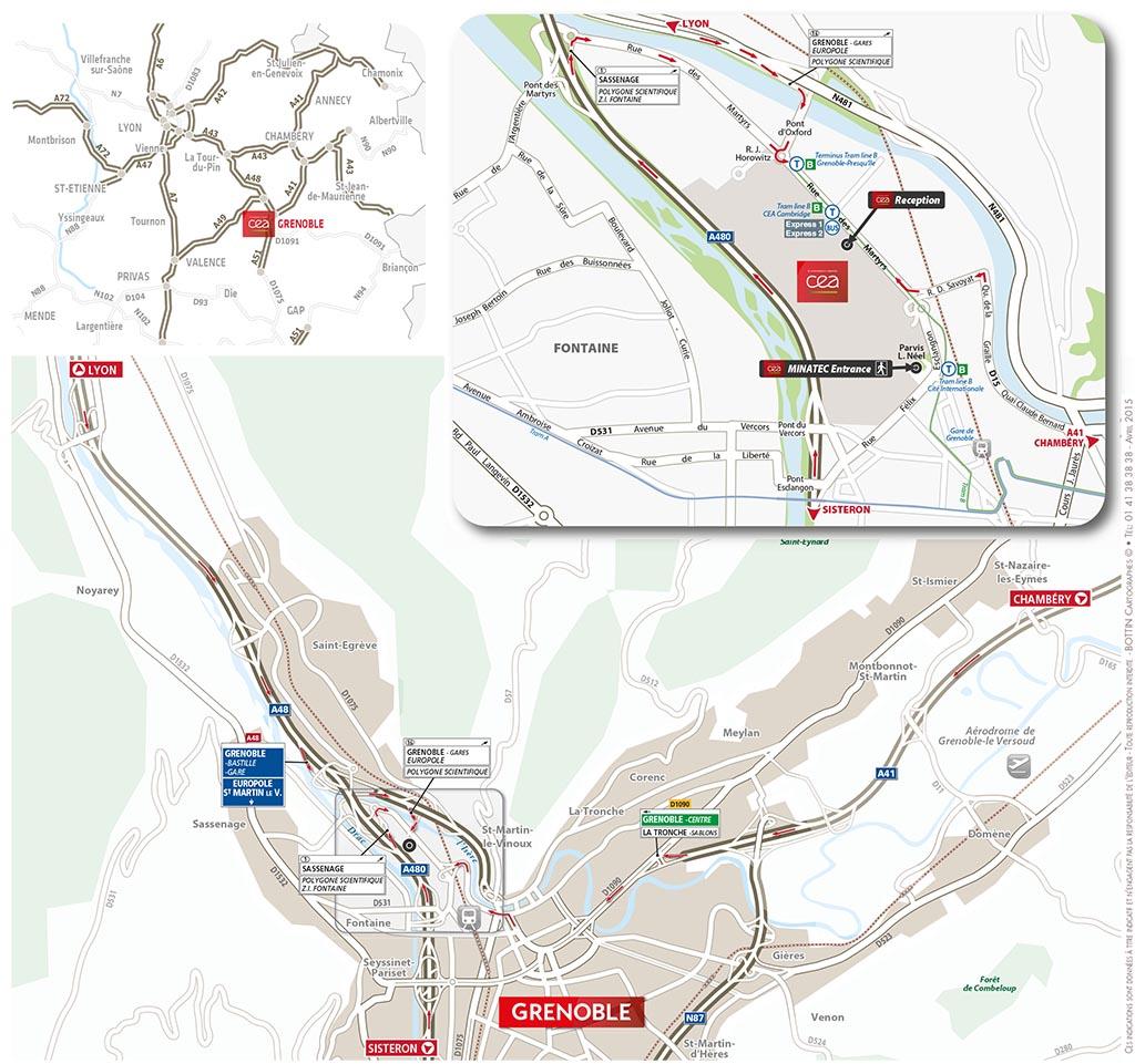
ACCESS BY PUBLIIC TRANSPORT:
From Gare de Grenoble:
Transisère Express 1 (direction Voiron):
CEA CAMBRIDGE STATION - Reception (10’).
Transisère Express 2 (direction Voreppe):
CEA CAMBRIDGE STATION - Reception (10’).
Tram line B (direction Grenoble Presqu’île):
CITÉ INTERNATIONALE STATION - MINATEC Entrance (10’)
or CEA CAMBRIDGE STATION - Reception (15’)
On foot, take the exit next to Europole, continue onto Avenue du Doyen L.
Weill and then use the MINATEC entrance at the end of the road (10').